China-developed EUV lithography could trial in 2025
 Cette publication existe aussi en Français
Chinese electronics giant Huawei is testing elements for an extreme ultraviolet (EUV) lithography machine at its Dongguan facility, according to two sources posting photographs on X social media.
The sources say the equipment is scheduled for trial production of circuits in 2Q25 with full-scale manufacturing in 2026, without attributing the information to any sources of their own. They add that the equipment is based on a laser discharge induced plasma (LDP) to produce light of 13.5nm wavelength.
The credibility of the timetable therefore remains uncertain although China is highly motivated to try and develop EUV lithography.
China has been denied access to the EUV lithography equipment from the monopoly commercial supplier, ASML Holding NV, for several years. This has been on the grounds that China could use advanced technology to develop AI and high-performance computing systems that would be used by the Chinese military. The export control has limited SMIC, China’s leading domestic foundry, to the manufacture of circuits at about 7nm or 5nm using deep UV immersion lithograpy with sub-optimal yield and efficiency. At the same time the world’s leading foundry, TSMC is manufacturing 3nm circuits and aiming for 2nm but is also under export license controls imposed by the US intended to prevent high-performance chips reaching China.
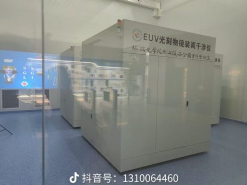
The image shown is of an optical interferometer, just one element of many needed to make an EUV scanner, a machine that is typically the size of a double-decker bus. A translation of the Chinese text on the side of the machine reads: “EUV lithography objective lens assembly and alignment interferometer. Changchun Institute of Optics, Fine Mechanics and Physics (CIOMP).
LDP is a lower-cost light source than the laser-produced plasma (LPP) used by ASML. The LPP is more difficult to manage but produces a higher output plasma, which corresponds to higher wafer throughput in the lithography machine.
It was previously reported that academics in China were working on soft x-rays as a light source for advanced lithography. This was clearly a long way short of a precisely tunable EUV scanner.
China’s synchrotron EUV lithography light source is no sanctions buster
Tests on interferometry for the positioning of the multiple reflective lenses that make up a EUV scanner appears to show China breaking free from dependence on the US and the western hemisphere in advanced chip making.
However, the complexity of bringing multiple subsystems together to form an EUV lithography scanner together with the necessity to develop a support ecosystem to provide pellicles, masks, and resist materials still means that China could be years behind getting to the leading-edge of chip manufacturing.
Related links and articles:
https://x.com/Ma_WuKong/status/1898380058856927278
https://x.com/zephyr_z9/status/1898015204103082441
News articles:
China’s synchrotron EUV lithography light source is no sanctions buster
China plans to build a giant chip factory driven by particle accelerator
Rapidus installs Japan’s first EUV lithography for 2nm pilot line
 If you enjoyed this article, you will like the following ones: don't miss them by subscribing to :