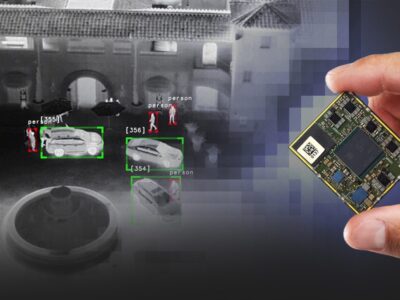
Synopsys ports Moortec PVT sensor to 3nm
Synopsys has ported its process, voltage and temperature (PVT) monitoring and sensing subsystem IP to TSMC’s 3nm process technology.
The PVT monitoring and sensing subsystem IP developed by recent UK acquisition Moortec provides real time data on the performance of next generation chips in key 3nm applications such as artificial intelligence (AI), data centre, high-performance computing (HPC), consumer and 5G. The deeply embedded PVT monitoring and sensing subsystem technology is used to assess key chip parameters both during production but also for measurement and analysis of real-time dynamic conditions during every stage of the device life cycle.
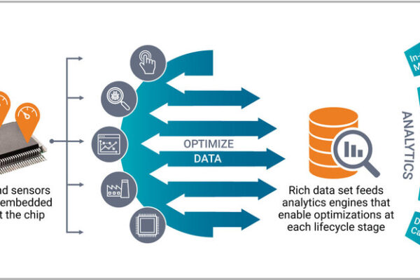
The in-chip sensing from Moortec, which is now a part of Synopsys, continues to be an essential element to achieve the highest levels of performance and reliability within today’s advanced process technologies, underpinning optimization schemes, telemetry, and analytics and is a foundational element of Synopsys’ Silicon Lifecycle Management (SLM) platform.
The SLM process begins with the placement of the in-chip sensors and PVT monitors deep within the chip. The data they provide facilitates a greater understanding of chip performance and power activity and enables the SLM platform’s analytics engines to drive more detailed and precise optimizations at each stage of the semiconductor lifecycle, from the early design phase, through in-field mission mode operation.
“TSMC continues to work with our ecosystem partners to address customers’ design challenges in power and performance and enable next-generation silicon innovation with design solutions using TSMC’s latest technologies,” said Suk Lee, vice president of the Design Infrastructure Management Division at TSMC. “The new Synopsys DesignWare PVT monitoring IP is a demonstration of the value of our ongoing collaboration with Synopsys and will allow continued product support for our mutual customers as they benefit from the power and performance advantages of TSMC’s N3 process technology.”
The modular design of the PVT subsystem developed by the Moortec engineers provides a fabric of PVT monitors that are highly configurable based on the target application. This latest solution for TSMC N3 process technology includes a distributed thermal sensor enabling highly localized thermal analysis, a new catastrophic trip sensor for programmable protection against thermal runaway and an additional thermal diode providing an independent measure of die temperature even when the chip is powered off. The whole system is controlled by a fourth-generation PVT controller which allows easy access to data from multiple instantiations of the individual embedded monitors and sensors.
“Driven by the demand for ever-increasing design complexity and device gate density, the adoption of PVT monitoring is now critical to successful advanced node chip design,” said Amit Sanghani, vice president of Hardware Analytics and Test Group at Synopsys. “The full suite of DesignWare embedded PVT monitors and sensors, part of Synopsys’ innovative new Silicon Lifecycle Management Platform, will offer the design community innovative in-chip sensing technologies, real-time deep chip insights, and enhanced product utilization throughout the silicon lifecycle.”
The DesignWare PVT monitoring and sensing subsystem can be configured to specific sector applications and is now available for early customer integration.
Related 3nm articles
- Multicore GPU aims for data centre designs
- TSMC certifies Synopsys and Cadence tools for N3 process
- Socionext taps Synopsys 5nm memory IP for datacentre AI
Popular articles on eenews Europe
- Europe looks to the end of the mobile phone
- Newport Wafer Fab faces Chinese takeover
- Snap buys UK smart glasses supplier for $500m
- Swiss centre aims for 100 qubit quantum computer
- Boom quarter for top 10 semiconductor companies
- 22 new 200mm fabs in capacity boom
 If you enjoyed this article, you will like the following ones: don't miss them by subscribing to :