Intel, TSMC both set to report on stacked CFETs at IEDM
Chipmakers Intel and TSMC are both scheduled to report on the development of vertically-stacked complementary field effect transistors (CFETs) at this year’s International Electron Devices Meeting (IEDM) coming up in December, in San Francisco.
The CFET is thought to be the transistor architecture to come after the gate-all-around multi-channel transistors. These are being adopted at the 3nm and 2nm nodes by chip manufacturing leaders TSMC, Samsung and Intel.
The idea of the CFET, where n- and p- type transistors are stacked vertically and monolithically, was proposed by the IMEC research institute back in 2018 (see IMEC presents ‘n-over-p’ complementary FET proposal). Since then numerous research papers have fleshed out the proposal but these have come IMEC and academic researchers rather than R&D teams at commercial organizations.
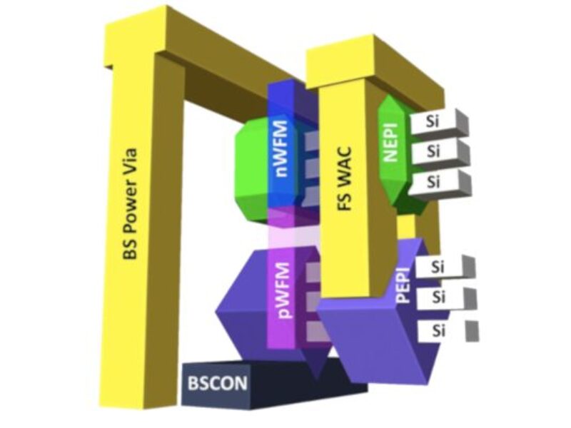
At the IEDM conference Intel researchers are expected to discuss a 3D monolithic CFET device that they manufactured that comprises three n-FET nanoribbons on top of three p-FET nanoribbons, with 30nm of vertical separation between them. They will present in paper 29.2: Demonstration of a Stacked CMOS Inverter at 60nm Gate Pitch with Power Via and Direct Backside Device Contacts.
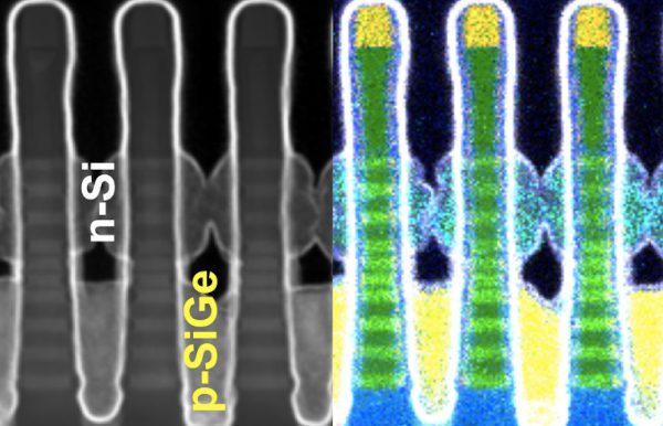
TEM micrograph of the Intel CFET device following vertically stacked dual source-drain epitaxy at CPP=60nm. Source: IEDM.
The CFET provides the obvious benefit of two transistors occupying the space of one in a GAA, FinFET or planar architecture. But it also means that CMOS logic circuitry can be designed more efficiently. IMEC has previously made the point that standard cell area is mainly dependent on access to transistor terminals and that CFETs can simplify this.
The Intel team are due to describe a industry first – fully functioning inverter test circuits in CFET – built at a 60nm gate pitch. The devices also featured vertically stacked dual-S/D epitaxy; dual metal work function gate stacks connecting the n- and p-transistors.
In addition Intel has include backside power delivery, an idea that was also proposed by IMEC and that is now part of the Intel roadmap for delivery in its Intel 20A – or 20 angstrom – manufacturing process.
The researchers also will describe a nanoribbon “depopulation” methodology for when unequal numbers of NMOS and PMOS channels are required. The work helps to increase the understanding of the potential to scale CFETs for logic and SRAM applications.
TSMC researchers have been allowed to submit a “late-news” paper in the same session: Paper 29.6 is entitled: Complementary Field-Effect Transistor (CFET) Demonstration at 48nm Gate Pitch for Future Logic Technology Scaling.
The team from TSMC will discuss what they describe as a practical, monolithic CFET approach for logic technology scaling on a 48nm gate pitch. Like Intel they are adopting an n-type nanosheet transistors above p-type nanosheet transistors. The paper will report on the on-state current and subthreshold leakage – described as “high” and “low” respectively in the precis of the paper. This leads to an on/off current ratio of six orders of magnitude. The on/off current ratio (six orders of magnitude).
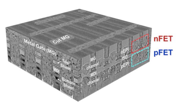
An inline cross-section transmission electron microphotograph shows TSMC’s monolithic CFET with a gate pitch of 48nm and with nFETs placed above pFETs, and both types of transistors surrounded by a single metal gate. Source: IEDM.
The transistors exhibited an FET survival rate of greater than 90 percent, according to the paper precis. A final comment in the precis is that: “While other essential features still must be integrated to unleash CFET technology’s potential, this work paves the way for that to happen.”
An inline cross-section transmission electron microphotograph shows a monolithic CFET with a gate pitch of 48nm and with nFETs placed above pFETs, and both types of transistors surrounded by a single metal gate.
Related links and articles:
News articles:
IMEC presents ‘n-over-p’ complementary FET proposal
IMEC maps out monolithic CFET at VLSI Symposium
IMEC semiconductor roadmap shows end of metal-pitch scaling
Stacked CMOS could overcome Forksheet limitations, says IMEC
 If you enjoyed this article, you will like the following ones: don't miss them by subscribing to :