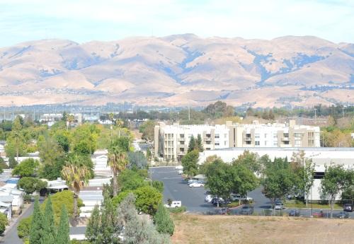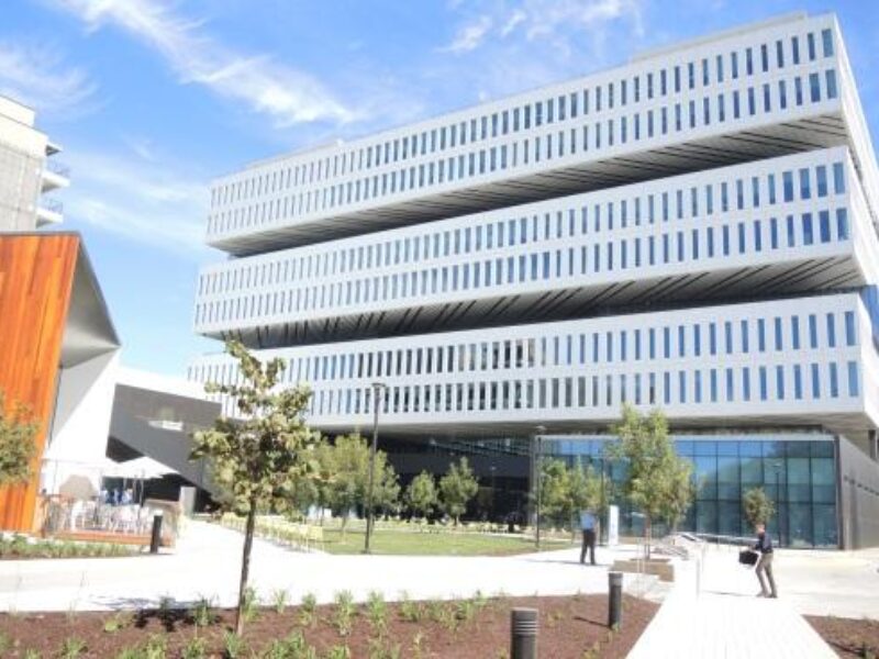
So it seemed fitting that on the clear day when Samsung opened its 10-story Silicon Valley office you could stand on the top floor and just pick out the giant cranes across town constructing Apple’s circular headquarters.
San Jose Mayor Sam Liccardo gave a nod to the rival in his comments to several hundred Samsung employees and guests at the opening. “Hello future denizens of spaceship Samsung, we look forward to seeing you take off in San Jose,” he said.
Indeed, the race continues. The giants have already logged several laps, leapfrogging each other with high profile smartphone and tablet features running on ever faster and more integrated SoCs.
Samsung came in first in the battle of the buildings, with more than 700 employees already inhabiting its 1.1 million square feet. Apple is still raising the walls of its new headquarters, though no doubt architects for both efforts can find reason to claim bragging rights.
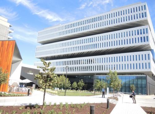
The new Samsung office costs about $300 million and will house research labs for semiconductors, LEDs and displays.
Both buildings stand out for their size and style, something that isn’t hard to do in the low slung solemnity of Silicon Valley office parks. Both in their own ways try to push the boundaries of architecture that encourages interaction, hoping for collaboration and unexpected innovations.
In my mind, the Samsung cube with its cut-through courtyard symbolizes the company’s relative openness. The Apple spaceship suggests the consumer giant’s more insular mystic.
The opening came the same day a Korean paper reported Samsung will cut by 20% it’s spending on capital equipment for semiconductors next year. Executives at the event decline to comment on the report, but even if it proves true it would be a slightly smaller cut than its other rival, Intel, is planning.
A spokesman for the company’s foundry business stuck to the corporate message that Samsung is ramping the 14nm process in which it is making its latest Exynos SoCs. It plans to have mass production on a 10nm node by the end of next year, using triple patterning on critical layers.
In many ways, the semiconductor race is an even more dramatic one than the higher profile smartphone slugfest. The billions Samsung spent on its Austin fab made it one of the largest foreign investments in the U.S. at that time.
Samsung’s fab complex in Giheung, South Korea will not be on the cover of Architectural Digest, but it is doing work fundamental to the success of many electronic products, including the iPhone. Such plants must continue to turn the crank on increasingly complex and expensive processes to fuel the new spaceships powering up in San Jose and Cupertino.
That said, my tour around the new headquarters for Samsung Device Solutions was punctuated by a few oohs and ahhs. I posted a handful of pictures on the following pages.
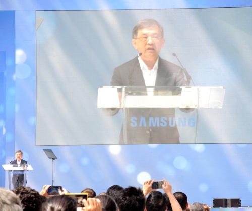
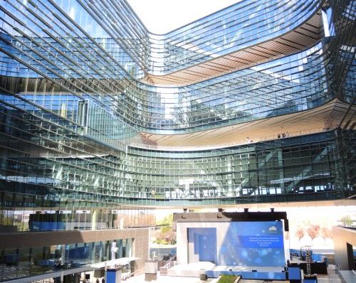
Oh-Hyun Kwon, CEO of Samsung Electronics (above), gave a $1 million STEM scholarship to San Jose State University to celebrate the opening on a stage set up in the building’s massive courtyard (below).
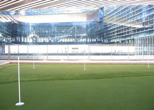
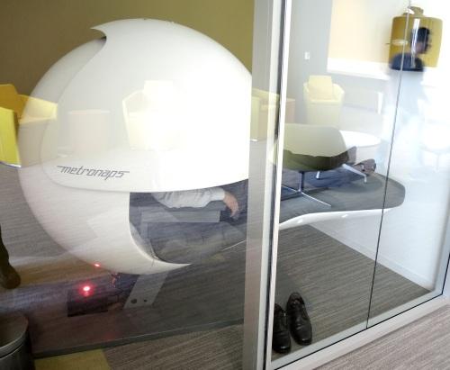
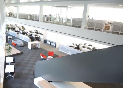
The hard-working Asian culture meets the laid back Silicon Valley way with an open fifth floor that sports putting greens (above) and a ground-floor lounge that includes private sleeping pods.
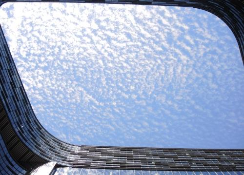
The views are fine whether you are looking directly up from the courtyard or out at Silicon Valley from the fifth floor.
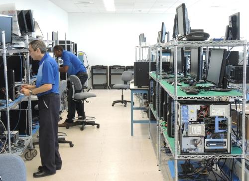
Yes there really are labs tucked away such as the one above on the tenth floor where solid-state drives are designed and tested as well as real Silicon Valley cubbyholes below.
About the author:
Rick Merritt is Silicon Valley Bureau Chief, EE Times
 If you enjoyed this article, you will like the following ones: don't miss them by subscribing to :
eeNews on Google News
