Samsung’s 14 nm LPE FinFET transistors
Samsung’s Exynos 8 SoC is receiving some press buzz as the company prepares to launch its 14 nm Low Power Plus (LPP) process that is an update to its current Low Power Early (LPE) process used in its Exynos 7 SoC and the Apple A9 SoC.
There are now three foundries capable of making finFET transistors: Intel, Samsung and TSMC. We at TechInsights last looked at Samsung’s 14 nm low power early (LPE) finFET process used in Exynos 7420 SoC in May of 2015 (Samsung Galaxy S6 Edge Smartphone). We were a little coy in our discussions of the process technology used to make the transistors; our business after all is to sell reports describing just this.
It is almost a year on now and there is talk of Samsung’s updated 14 nm LPP finFET process. We won’t know the details of this process until we get our hands on some samples of either Samsung’s Exynos 8890 SoC, or Qualcomm’s Snapdragon 820 SoC later this spring, but we can reveal more of the 14 nm LPE process technology used in the Exynos 7420.
We begin with a tilt view SEM image of a typical Samsung 14 nm LPE finFET transistor in Figure 1. The transistor channels are formed as silicon fins than run from the lower left to the upper right of the photograph. The fins are buried under dielectrics and are not visible, so we have drawn arrows to indicate their orientation. The metal gates lie in the orthogonal direction, wrapping over the sides and tops of the fins. Large source and drain (S/D) contacts are seen on either side of the gate electrodes.
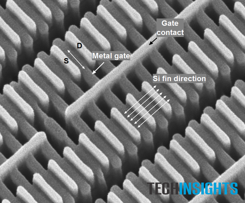
Figure 1: Tilt view SEM image of Samsung 14 nm FinFET transistors (Source: , TechInsights)
The layout of the gate and fins is perhaps more clearly seen in Figure 2 of another set of Samsung finFET transistors, which is a plan view SEM image of a few FinFET transistors. Four silicon fins are aligned in a vertical direction, underneath the metal gates that run in the horizontal direction. The two transistor structures are surrounded by a well contact ring, that serves to isolate them from the rest of the circuitry on the die.
The fins have a 49 nm pitch that require a double patterning process to make them. There are two choices: litho-etch litho-etch (LELE) that Intel is believed to be using, or self-aligned double patterning (SADP). We think Samsung is using the LELE process to pattern these fins. An additional mask and litho process is required to cut the ends of the transistors.

Figure 2: Plan view image of Samsung 14 nm FinFET transistors (Source: , TechInsights)
Figure 3 is a TEM cross section of a typical NMOS transistor used by the Exynos 7420, and we note that the roughly 30 nm measured gate length is nowhere close to the claimed 14 nm process node and this is true for both Intel and TSMC as outlined in Table 1. We will discuss this later.
The transistor gates are fabricated using a replacement gate process. This involves depositing a sacrificial layer, typically polysilicon, patterning and etching to form approximately 30 wide stripes. These stripes will define the transistor gate lengths.
Sidewall spacers (SWS) are then formed along the sides of the gates, and these are used for the recess etch definition and subsequent epitaxial grown of Si for the NMOS transistors (eSi) and SiGe (eSiGe) for the PMOS transistors. After completing the source/drain formation, the cavities are filled with oxide, followed by a chemical mechanical planarization (CMP) process.
The SiGe in the PMOS source/drain regions has a larger lattice constant that the surrounding Si fin and this puts compressive strain on the PMOS transistor, boosting its drive current. The heavily doped SiGe and the NMOS eSi source/drains also wrap around the sides of the fins to provide a larger contact patch for the tungsten filled contacts, yielding lower contact resistances to the transistors.
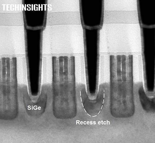
Figure 3: Samsung 14 nm Node PMOS Transistor (Source: , TechInsights)
At this point, the sacrificial gates are removed and the gates are filled with their gate dielectrics and metals.
We show the metal fills for the NMOS and PMOS transistors in Figure 4, where the two gates lie overtop a region of isolation. The transistors share a common HfO/oxide high-k gate dielectric stack. The HfO is quite dense and shows up as the dark band lining the outside edges of the transistor. The gate oxide layer lines the outer surface of the HfO.
The inner surfaces of the HfO are lined with the NMOS and PMOS work function metals that are used to set the threshold voltages of the transistors, and these metals have different compositions.
The gate fills are somewhat different as well. We see the inner most portion of the NMOS transistor being lined with TiN and filled with W, but not the PMOS transistors. The absence of W in the short gate length PMOS transistor is due to the TiN closing off the top of the gate, preventing the W fill. This necking off of the PMOS gate also gives rise to the void seen near its bottom. The W reappears in long gate length PMOS transistors where the tops of the gates are not necked off by the TiN.
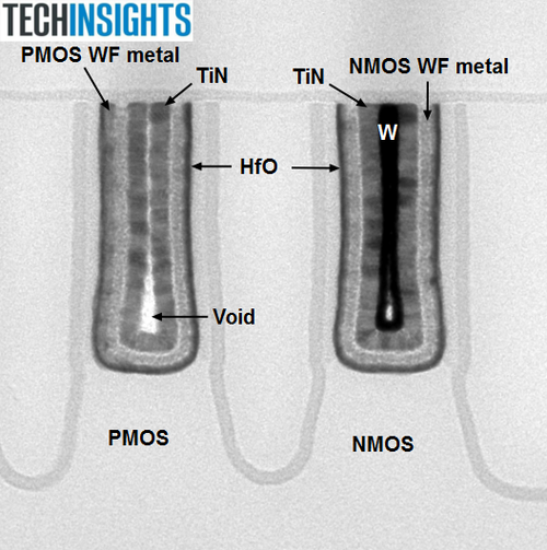
Figure 4: Dummy NMOS and PMOS Transistors (Source: TechInsights)
We had alluded earlier to Samsung’ FinFET transistor being much longer than the stated process node. They are not alone in this as both Intel, and TSMC sport finFET gate lengths longer than the process node (Table 1 below). In fact, there is not much in the way of lithographic sizes that are the same as the declared process node. How can this be?
Table 1: Selected Transistor Dimensions for Samsung, Intel and TSMC
| Feature | Samsung 14 nm | Intel 14 nm | TSMC 16 nm |
| Fin pitch (nm) | 48 | 42 | 45 |
| 1/3 fin pitch | 16 | 14 | 15 |
| Gate length | ~30 | ~24 | ~33 |
| Contacted gate pitch (nm) | 78 | 70 | 88 |
| Minimum metal pitch (nm) | 67 | 52 | 70 |
| 6T SRAM cell area (µm2) | 0.08 | 0.059 | 0.074 |
(Sources: , Logic Detailed Structural Analysis of the Intel 14 nm 5Y70 Processor, TSMC 16 nm finFET Process in Apple A9 Processor Logic Detailed Structural Analysis, TechInsights)
Figure 5 provides a clue. We have plotted both the physical gate length that we have measured for a number of advanced logic devices vs. the manufacture’s claim process node, along with the contacted gate pitch of the transistors. Transistors fabricated at the 130 nm process node and larger exhibit gate lengths that about the same as the process node. But from about the 110 nm down to the 65 nm node, the gate lengths shrink faster than the process node, being shorter than the process node. The rate of gate length shrinkage has slowed for the 45 nm and smaller process nodes.
We have also plotted the contacted gate pitch for the same devices, and this pitch is about 3.3 times that of the process node, and is consistent for all of the process nodes. We also find that the minimum metal pitch also scales as approximately 3X process node.
We often use the contacted gate pitch and 6T SRAM cell area as proxies for the process node; which raises questions as to whether a claimed 16 nm or 14 nm process node is really the node. For example, Samsung’s fin pitch, gate length, contacted gate pitch and 6T SRAM cell are all larger than Intel’s 14 nm process, and its 6T SRAM cell area is bigger than TSMC’s 16 nm SRAM. So is it really a 14 nm process?
One of our engineers has suggested that the fin pitch is a proxy for the process node, much like we see with the active pitch in DRAMs and STI pitches in NAND flash memories. We list the 1/3 fin pitch in Table 1 for the Intel, Samsung and TSMC 16/14 nm node devices, and indeed this is not a bad proxy for the process node.
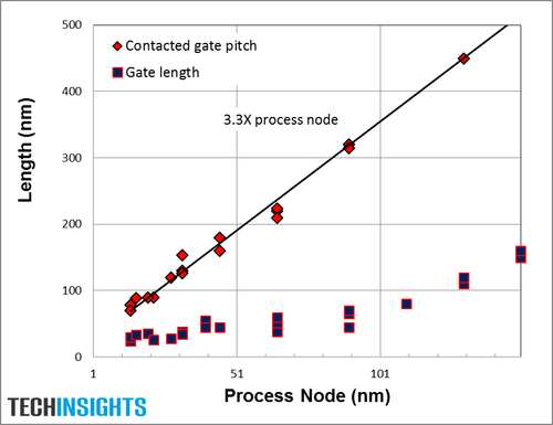
Figure 5: Transistor Gate Length and Contacted Gate Pitch vs. Process Node (Source: TechInsights)
What should we expect for their 14 nm Low Power Plus (LPP) process? Samsung’s recent press releases suggest that the LPP process will feature a 15% increase in the transistor switching speed and a 15% power consumption decrease. These are being achieved by increasing the transistor’s fin height and enhanced strain engineering. For me, I am anticipating a bit of a process shrink as well to bring the transistor and 6T SRAM cell sizes closer to that of Intel.
For now, we will bide our time until the Exynos 8 SoC or Snapdragon 820 SoC are released in the next generation of Apple and Samsung Smartphones.
About the author:
Kevin Gibb, Product Line Manager, TechInsights.
 If you enjoyed this article, you will like the following ones: don't miss them by subscribing to :