AlN nanowall-based UV LEDs boast 60% internal quantum efficiency
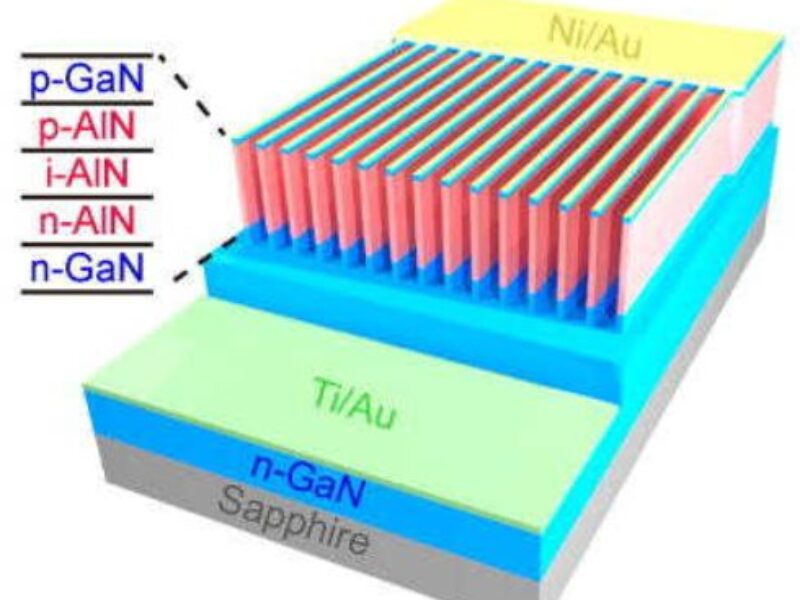
The AlN nanowall LED stacks were built on top of GaN nanowall structures which were first created on an n-type GaN template on a sapphire substrate using e-beam lithography and dry etching techniques. Grown through molecular beam epitaxy (MBE), the AlN nanowall LEDs then consisted of Si-doped AlN, non-doped AlN, and Mg-doped AlN segments, with each layer being approximately 40nm thick. A 3nm p-GaN layer was deposited on the top surface to serve as p-contact with Ti/Au n-metal.

a GaN template on a sapphire substrate.
Prior to growing the AlN nanowall LEDs, a 300 nm thick SiOx layer was first deposited on the GaN nanowall structures for surface passivation and electrical isolation, then p-Metal Ni/Au contacts were deposited through selectively etched areas.
The paper “Molecular beam epitaxial growth and characterization of AlN nanowall deep UV light emitting diodes” published in the Applied Physics Letters details various experiments with wall widths varying from 100nm to 1μm, noting a consistent blueshift in the emission wavelengths which the researchers explain by the reduced tensile strain distribution.
In their paper, the researchers report devices with nanowalls as long as 120 μm, exhibiting excellent current-voltage characteristics, including a turn-on voltage of 7V and current densities of over 170A/cm2 at 12V (when fabricated with a wall width of 410nm).
“Compared to conventional nanowires, nanowall structures exhibit well controlled geometry and are ideally suited for the fabrication of large area devices. Moreover, TM polarized light emission can be efficiently extracted from the lateral surface of nanowall structures” they write.
Another observation the researchers made was that AlN nanowall LEDs of narrower widths showed much higher injection current density. They attributed this to the reduced defect distribution and a more efficient Mg-dopant incorporation in AlN nanowall arrays with narrower widths.
These nanowall structures could become an interesting building block for achieving high performance deep UV optoelectronic devices.
Related articles:
UV LED market on a 34% CAGR between 2015 and 2020, predicts TrendForce
Bavarian project to develop AlN wafers for AlGaN UV leds
UV LEDs: solving the droop issue
Better light extraction for deep UV leds
 If you enjoyed this article, you will like the following ones: don't miss them by subscribing to :