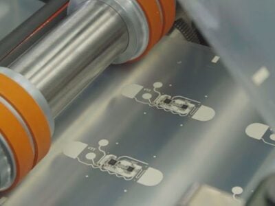
SOI wafers optimized for NIR, 3D imaging
The wafer enables increased performance in the near-infrared spectrum including 3D image sensors such as those used in the latest smartphones for augmented and virtual reality applications and facial recognition.
The Imager-SOI provides enhanced quantum efficiency by trapping light above the buried oxide (BOX) layer and reduces cross-talk between pixels. The BOX also limits the impact of substrate noise and metal contamination, and acts as a diffusion barrier to prevent metal contaminants migrating into pixels.
The net result is an improved signal-to-noise ratio in the NIR spectrum, the company claimed. Wafers are available at 300mm diameter.
Market research firm Yole Developpement forecasts that the annual market for 3D imaging and sensing devices will grow with a compound annual growth rate of 37.7 percent over the five years from 2017 to reach $9 billion in sales in 2022.
Related links and articles:
News articles:
Could ST ToF sensor lead to Apple 3D camera?
Rising SOI tide lifts Soitec into profit
Soitec launches FDSOI pilot line in Singapore
OmniVision enhances near-infrared image sensing
 If you enjoyed this article, you will like the following ones: don't miss them by subscribing to :