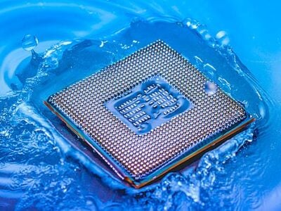
UMC to pay big price for Fujitsu foundry
The company has been prepared a high price to acquire the remainder of the wafer fab because demand for mature processes manufactured on 300mm wafers is high and UMC reckons it is saving itself the billions of dollars and time it would cost to build a new wafer fab. The deal is set to conclude on January 1, 2019, subject to the approval of government authorities.
Mie Fujitsu Semiconductor (MIFS) is a 300mm wafer fab set up as a subsidiary of Fujitsu Semiconductor Ltd. to operate as a pure-play foundry. In 2014, Fujitsu and UMC concluded an agreement for UMC to acquire a 15.9 percent stake in MIFS through progressive phases. In addition, MIFS has been licensing UMC’s 40nm CMOS manufacturing process and establishing a 40nm logic production line.
MIFS will become a wholly-owned subsidiary of UMC although the name and details of distribution after the deal goes through are yet to be determined. For the present, MIFS will maintain its existing distribution channels for customers.
Jason Wang, co-president of UMC said, “UMC is experiencing high demand from mature 12-inch processes. With new applications in 5G, IoT, automotive and AI requiring these technologies, we anticipate the market conditions driving this demand to remain strong for the foreseeable future. The acquisition of a fully qualified, equipped, and volume production proven 12-inch facility provides greater time and ROI advantages compared to building a fab from scratch, which would cost several billion dollars and several years to construct and equip.”
Related links and articles:
News articles:
Fujitsu is licensee of Nantero’s carbon-nanotube RAM
Renesas seeks purchasers for fabs
Tower buys three wafer fabs for $8 million
 If you enjoyed this article, you will like the following ones: don't miss them by subscribing to :