EUV not needed at 10 or 7nm, says Intel
It also gave its most detailed look to date at its foundry service for sharing its chipmaking prowess, including a description of a new low-cost alternative to 2.5D chip stacking it has in development.
“My day job is working on [research for a process to make] 7 nm [chips and] I believe there is a way without EUV,” said Intel fellow Mark Bohr, responding to a question after a talk on Intel’s new 14 nm process.

The optimism is significant given the core lithography used for patterning chips hasn’t had an upgrade in more than a decade. Chipmakers generally don’t expect the much-delayed extreme ultraviolet (EUV) lithography in time for 10 nm chips, but many still hold out hopes it could be ready for a 7 nm generation.
“I am very interested in EUV [because it] could really help scaling and perhaps process simplification, reducing three or four masks to one in some cases,” Bohr said. “Unfortunately, it’s not ready yet — the throughput and reliability are not there.”
Bohr did not give any hints about how Intel will make 7 or even 10 nm chips without EUV. However he did note at 14 nm Intel is using triple patterning on one or more critical layers.
Although wafer costs rose at an accelerating rate for the last two nodes due to the need for more masks, Intel continues to pack more transistors in a given area of silicon. The density offsets wafer costs, leading to the cost-per-transistor decline, Bohr said in his talk on Intel’s 14 nm process.
“One of the fundamental benefits of Moore’s Law is smaller feature sizes, primarily to get lower cost per transistor so we can do more things” in a similarly sized chip, he said.
Intel already announced it has started making in volume chips using a 14 nm process at a lower cost per transistor than its prior 22 nm generation. It also said it is in development of a 10 nm process that it believes will deliver lower cost per transistor.
In a separate talk, Intel said before the end of 2015 it could offer external foundry customers a chance to try out its emerging 10 nm process on shared wafers called shuttles.
In his most detailed talk to date, Sunit Rikhi, general manager of Intel’s custom foundry business, described the details of an end-to-end service that’s now more open than ever but still evolving.
Customers are currently using their own designs, supplemented with some IP blocks from Synopsys and Cadence. In the future, Intel will offer some IP, starting with an Atom core still in development.

“Today we do not have an [Intel] IP catalogue. We know there is a large amount of energy to make truly pluggable IP in the form customers are used to, and we have started giving it the engineering focus it needs,” said Rikhi.
Users can design with customer-owned tooling or choose from third-party tools from Ansys, Cadence, Mentor Graphics, and Synopsys that Intel has qualified. Each step in the flow varies, with sometimes only one and sometimes several tool choices available.
The foundry’s initial 22 nm offering comes in just one flavor. Starting at 14 nm, Intel is offering general-purpose and low-power flavors with a family of transistors geared for high performance or low leakage needs.
Intel will provide a wide range of engineering services including chip design, packaging, and use of its in-house designed testing systems. The company recently revealed it builds its own chip test systems and test methods in house, claiming it shaves in half costs of using external gear.
“It’s a very significant benefit, and more than a cost reduction; it’s a systematic interface… for testing increasingly complex products in an engineering lab and taking them quickly to production,” Rikhi said.
The company has two customers now in volume production with a third ramping. It has more than the six customers it has publicly announced, including one that signed on after the announcement of Panasonic in July.
“Our ability to keep cost of transistors going down by more than the normal area scaling is unique, and our customers appreciate it,” said Rikhi.
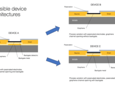
Most significantly, Intel is far along in testing a lower-cost alternative to 2.5D chip stacks it calls the Embedded Multi-Die Interconnect Bridge.
Unlike the 2.5D process, EMIB does not lay dies side-by-side on large silicon interposers, connecting them with through silicon vias (TSVs). Instead it uses a more conventional kind of flip chip process with metal bump interconnects inside a package.
EMIB employs back-end-of-line metallization and wafer thinning techniques used in a 2.5D stack. However by eliminating TSVs it significantly reduces costs, including costs of wasted die, Rikhi said. The process offers interconnects that are as dense and fast as TSVs, he added.
Intel has prototyped chips with “far north of five die” linked in an EMIB package. It expects to sample the technique to foundry customers in 2015.
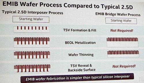
EMIB is less costly than 2.5D stacks, with no loss in interconnect density or speed, according to Sunit Rikhi.
Interestingly, Rikhi said Intel currently has nothing in development for foundry customers interested in creating memory stacks using so-called high bandwidth memory such as Micron’s Hybrid Memory Cube.
If Intel’s claims are true, it is reaping benefits at levels few others in the industry expect to see, a fact that could fuel its emerging foundry business and further widen its lead over competitors. Nevertheless, analysts gave Intel’s emerging foundry service mixed reviews.
Intel’s foundry costs are still unknown outside its current customers and may carry a steep premium over existing foundries, said Richard Doherty of Envisioneering. In addition, he noted only two customers are now in volume production through the effort started several years ago.
“One thing they don’t talk about is parametric yields,” said Handel Jones, principal of International Business Strategies. “It took them 18 months to address that” at the 14 nm node.
However, Jones added, “We still think they have an 18- to 24-month lead on other foundries in terms of manufacturing high volumes with reductions in cost per transistor.”
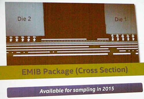
Another look at an Intel EMIB design.
Related articles:
Intel buys stake in ASML to boost 450-mm, EUV R&D
EUV still promising on IMEC’s road map
EUV firms to partner to speed up source improvements
 If you enjoyed this article, you will like the following ones: don't miss them by subscribing to :