Quantum transistor harnesses new effect
"We found that when deposited in a flat sheet just three atoms thick, our crystalline lattices exhibited a new electronic effect we call the quantum spin Hall effect," professor Xiaofeng Qian told EE Times.
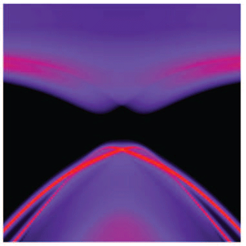
Topological phases in the two-dimensional transition metal dichalcogenide (TMDC) can be turned on and off by simply applying a vertical electric field shown here by the red crossing lines that conduct electricity along the edges of the material when the electric field is turned off. When the electric field is turned on the red lines are broken and a black gap appears between the valence and conducting bands of TMDC, which indicate the edges no longer conduct. (Credit: Qian et. al.) (Source: Texas A&M University)
In bulk topological materials like, the transition metal dichalcogenide (TMDC) used here, they conduct on the top and bottom, but are insulators in their interiors. What Qian and colleagues discovered was that when thinned down to just three-atomic-layers thick, they conducted only on the edges and not in the middle. What’s more their conduction could be switched — turned on and off with a gate — like a normal FET just by applying a perpendicular electrical field. Even more unusual, making the TFET a spintronic device, was that the electrons conducting along the edges traveled in different directions depending upon their spin.
"What’s more the electrons with up spin flow in one direction, while those with down spin flow in the opposite direction. So by controlling the injection of charged carriers, we can create a spintronic transistor," Qian told EE Times.
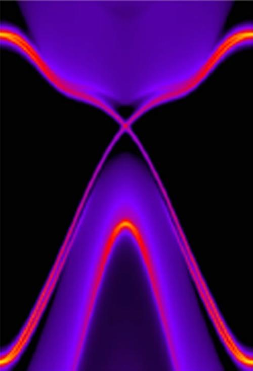
2-D topological insulators conduct only at their edges when cast as monolayers. There’s a black gap between the purple blobs at the bottom and top. The crisscrossing reddish lines that bridge the gap. The lines indicate the edge state of the material, allowing electrons to cross the gap and conduct electricity. (Credit: Qian et. al.) (Source:Texas A&M University)
Along with Qian, the science team consisted of researchers Ju Li, Liang Fu, Xiaofeng Qian, and Junwei Liu, experts in topological phases of matter and two-dimensional materials, at MIT. Plus supercomputer experts at TACC who help confirm their results by running the Vienna Ab initio Simulation Package on their Stampede and Lonestar supercomputers. The supercomputers were made available to the MIT team under the Extreme Science and Engineering Discovery Environment (XSEDE) funded by the National Science Foundation (NSF).
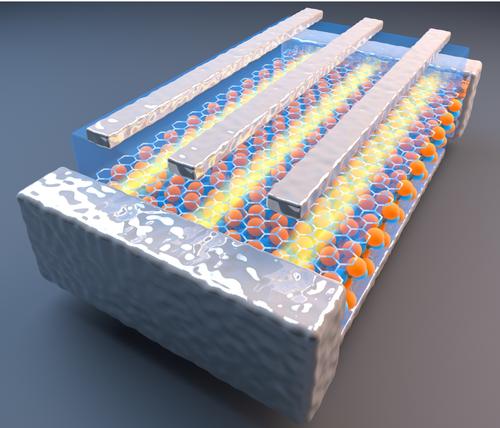
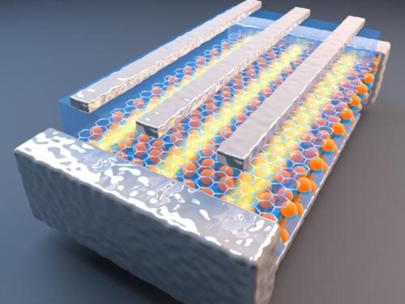
Artist’s rendering of quantum transistor, consisting of 2-D material "sandwiched" between boron nitride (gray). When an electric field is applied to the rectangular "gates" at top, it switches the quantum state of the middle layer (yellow) on and off. The boundaries of these "switched" regions act as perfect quantum wires, potentially leading to new electronic devices with low losses. (Credit: Yan Lian, MIT.) (Source:Texas A&M University)
Next Qian and colleagues want to hunt for new materials that exhibit the same or similar characteristics operating at room temperature. He is also handing off his theoretical work to several experimental labs which will build the new TFET in the lab. By combining the TFET with superconductors, Qian hopes experimentalists will achieve the Majorana fermion zero mode — the holy grail of topological quantum computing.
"There is so much opportunity in two-dimensional materials research. Its not just graphene we should be studying, but the many other opportunities in 2-D materials. We expect to be using 2-D materials in real applications in the very near future."
Funding was provided by the U.S. Department of Energy and the NSF.
— R. Colin Johnson, Advanced Technology Editor, EE Times
Professor Xiaofeng Qian,
principle scientist on
the project in the Department
of Materials Science and
Engineering at Texas A&M
University. (Source: Texas A&M)
 If you enjoyed this article, you will like the following ones: don't miss them by subscribing to :