Researchers pin-point quantum light emission from 2D materials
So far, the quantum emitters (QEs) had been assigned to both defects and strain gradients, mostly unwanted and unpredictable.
In a recent paper published in Nature Communications under the title “Large-scale quantum-emitter arrays in atomically thin semiconductors”, researchers from the University of Cambridge (UK) together with scientists from Harvard University (US) demonstrated how they were able to localize the sources of single photons by tuning the topography of such 2D materials.
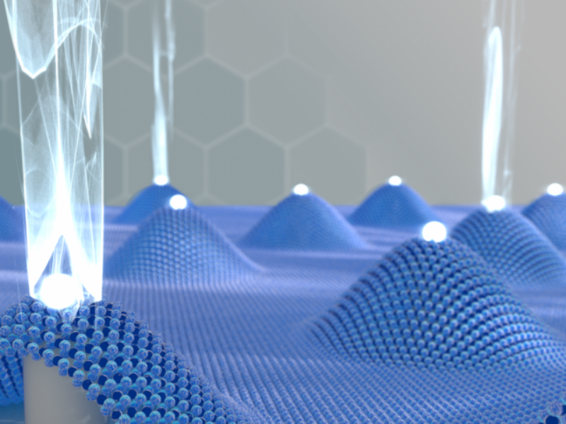
The paper discloses how by placing the active material (a monolayer of exfoliated WSe2 or WS2) on top of nanopillars regularly spaced apart, the researchers obtained an array of tent-shaped peaks distributed across the monolayer, forming localized physical disturbances from which single photons were emitted.
SiO2 nanopillars, 150nm in diameter and ranging from 60 to 190nm in height, were first created onto a silica substrate to form an array with a 4µm pitch (using a high-resolution direct-write lithographic process).
By placing tungsten diselenide and tungsten disulphide monolayers on top of such arrays (using an all-dry viscoelastic deposition process), the researchers created deterministic arrays of hundreds of QEs emitting across a range of wavelengths in the visible spectrum (610–680 nm and 740–820nm respectively).

from quantum dots in supported layered
semiconductors.
Credit: Pawel Latawiec/Harvard University.
In their paper, the researchers explain that the localized deformations created by the nanopillars result in the quantum confinement of excitons.
They also found these QEs to emit with a greater spectral stability than their randomly occurring counterparts, typically with bright sub-nanometre linewidth emission peaks. Increasing the nanopillar height also reduced the spread in the number of peaks arising at each nanopillar location, which leads the paper to conclude that the QEs’ optical emission could certainly be tuned by varying the shapes of the underlying nanostructures. In this case, the researchers extrapolate that MEMS or piezoelectric tuning could possibly allow dynamically tuned QEs for their integration into photonic structures.
They also predict that this novel way to create quantum emitters QE should not be restricted to a specific layered material but could be explored across many other 2D materials
Related articles:
LED features single photon emission
Breakthrough boosts 2D semiconductor photoluminescence
Thinnest-known LEDs open up new miniaturization horizons
 If you enjoyed this article, you will like the following ones: don't miss them by subscribing to :