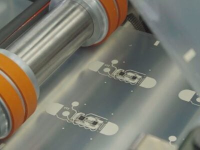
Samsung launches 7nm EUV process, SAFE partnership
The 7LPP (low-power plus) process is manufactured using extreme ultraviolet (EUV) lithography technology for wafer production and customers can now work with the Samsung Advanced Foundry Ecosystem (SAFE) partners to produce designs. The partners include Ansys, Arm, Cadence, Mentor, SEMCO, Synopsys and VeriSilicon and they can offer process design kits (PDK), IP cores, reference design flows, packaging and design services.
Compared to 10nm FinFET process, the 7LPP technology delivers up to a 40 percent increase in area efficiency with 20 percent higher performance or up to 50 percent lower power consumption, Samsung claimed.
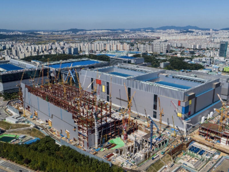
The initial EUV production has started in Samsung’s S3 Fab in Hwaseong, Korea. By 2020, Samsung expects to secure additional capacity with a new EUV line for customers who need high-volume manufacturing for next-generation chip designs.
“In collaboration with these ecosystem partners, we have established the necessary design enablement collateral to facilitate customer design starts on our differentiated 7LPP process,” said Jaehong Park, senior vice president of foundry design at Samsung Electronics, in a statement.
Samsung said there is a range of silicon-proven IP available including embedded memories and logic libraries and interface IP solutions including HBM2/2E, GDDR6, DDR5, USB 3.1, PCI Express 5.0 and 112G SerDes.
“ARM’s Artisan physical IP and POP IP acceleration technology, which enables 3GHz-plus compute performance on ARM’s latest cores, leverages the EUV benefits available on Samsung’s 7nm LPP process technology,” said Gus Yeung, general manager of ARM’s physical design group, in the same statement.
“Being one of the earlier adopters of 10LPP with volume production, VeriSilicon taped out a chip on 7LPP EUV and saw significant advantages in both performance and power consumption over 10LPP, and are ready to provide design service for our customers,” said Wayne Dai, CEO of Verisilicon in the same statement.
Related links and articles:
News articles:
Samsung early with 7nm process, says report
Apple describes 7nm A12 Bionic chip
GloFo rethinks its future, drops 7nm FinFET
 If you enjoyed this article, you will like the following ones: don't miss them by subscribing to :