Intel Fellow discusses high-NA EUV lithography progress
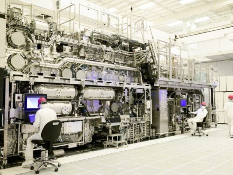
Intel has completed the assembly of the first high numerical aperture (high NA) extreme ultraviolet lithography scanner and Intel Fellow Mark Phillips discusses progress and prospects.
ASML Holding NV (Veldhoven, The Netherlands), the supplier of the Twinscan EXE: 5000, has to finish integration and calibration of the scanner, which is located at Intel’s R&D site D1X in Hillsboro, Oregon. Intel will begin development work on the machine later in 2024, said Mark Phillips, Intel Fellow and director of lithography, hardware and solutions for Intel Foundry logic technology development.
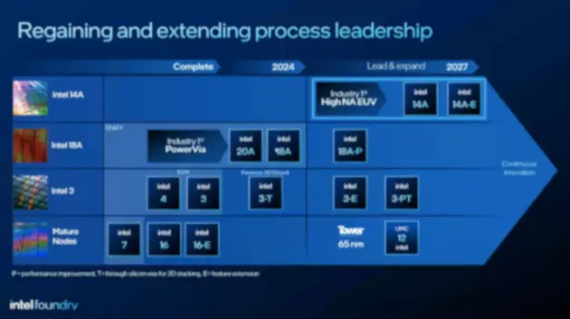
Intel expects to use both 0.33NA EUV and 0.55NA EUV alongside other lithography processes in developing and manufacturing advanced chips, starting with product proof points on Intel 18A in 2025. This will then move on to Intel’s 14A process in 2026, according to materials shown by Intel.
Process roadmap to 2027. Source: Intel
Phillips was speaking on a conference call with journalists to discuss high-NA EUV. High NA EUV is expected to be able to print features up to 1.7x smaller than existing EUV tools. This will enable 2D feature scaling, resulting in up to 2.9x more density. Compared to 0.33NA EUV, High NA EUV (or 0.55NA EUV) can deliver higher imaging contrast for similar features, which enables less light per exposure, thereby reducing the time required to print each layer and increasing wafer output.
Three nodes?
Phillips indicated he expects high-NA to address leading-edge chip manufacturing down to 1 angstrom and below which is essentially the dimensions of single atom.
“It [high-NA] is going to go several generations. How many nodes partly depends on how you define nodes. I expect at least three generations of high NA.” Phillips said that he did not foresee a reduction of EUV wavelength from the present 13.5nm as a way forward for lithography any time soon.
“Moving to a wavelength of 6.7nm brings a lot of other problems,” said Phillips. He said the optical requirements “explode” meaning they take up a lot more space. “The next discussion is likely to be about hyper-NA,” said Phillips saying there were certain possibilities around moving to an NA of 0.75. “Half-field tools with NAs at 0.75 could done largely with the technology developed so far and at a similar system size.”
However, the half-field size also indicates one of the issues around high-NA EUVL, which may feed into the adoption of chiplet component packaging.
With the implementation of high-NA optics, the maximum field size of the reticle is reduced due to the use of an anamorphic lens array. Specifically, the standard reticle limit is halved from 26mm by 33mm for conventional EUVL to 26mm by 16.5mm. This reduction is a result of the increased resolution capabilities of high-NA EUV lithography.
Stitching required
Phillips was asked if the reduced reticle size meant smaller die.
Phillips said: “Disaggregation, smaller die and chiplets is one way to go. But some customers will still want larger die so we will be offering a “stitching” capability. Right now it is not completely transparent to the designers.” Phillips added that Intel was working with EDA companies to try and make it easier to implement.
He added that it is important to be able to stitch design elements together to create single die to gain the maximum utilization of the expensive tool.
The price of the high-NA EUV exposure machine is said to be about US$380 million or more than twice the approximately US$180 million of the previous generation lower-NA EUV machines.
Related links and articles:
News articles:
Intel video shows high-NA EUV lithography machine installation
IMEC claims high-NA EUV patterning is ready to make chips
IBM teams for 2nm, 1nm EUV mask development
Canon could ship nano-imprint lithography machines in 2024
China’s synchrotron EUV lithography light source is no sanctions buster
 If you enjoyed this article, you will like the following ones: don't miss them by subscribing to :