Nanusens looks to £10m Series A round
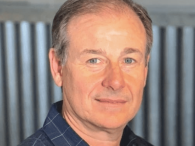
MEMS chip maker Nanusens is looking for a lead investor to raise £10m at a valuation of £40m, says its new chairman, Dr Graham Hine.
He has been brought into bring semiconductor expertise to the board and also invested in the seed round. He started out at Mullard (Philips Semiconductor) and is an investor is several semiconductor startups.
“The main priority is to raise Series A funding. We raised a bridging round of £2.3m a few months ago,” he told eeNews Europe. “We are looking to raise £10m on a pre money valuation of £40m and we are looking for a lead investor, and we are talking to potential investors. That will get us into revenue.”
“Most UK VCs are not very technical, and you really need someone in the VC who has an understanding of CMOS manufacturing and what Joseph is doing with MEMS,” he said.
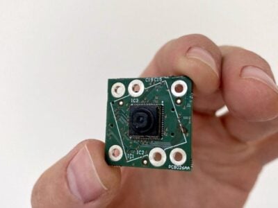
Nanusens is using standard CMOS process technology at foundries such as SMIC, TSMC and Globalfoundries to build MEMS devices inside a chip. It then has reactors in-house to release the MEMS structures using HF acid.
“To begin with we need to start making products as the proof of IP,” said Hines.
A key part of the fundraising is the company’s first patent in the US.
“We held off filing so that we could do a suite of patents simultaneously as this comprehensively covers and protects our technology in one go,” said Hine. “This is much safer than doing them one at a time as rivals could devise patent workarounds once they read each patent. That will be incredibly difficult now with our blanket protection of every aspect of our innovative nanotechnology.”
“Patents are valuable assets for the company. Having the patents in process and working NEMS in the lab are the two milestones that investors told us that we needed to achieve in order to start our Series A funding so we have officially started that.”
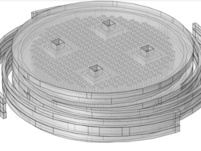
The patent covers a round MEMS device with a diameter of less than 150 microns with three evenly distributed springs that are spiral so that they can be long to give high sensitivity.
This design can be used by Nanusens in a number of its sensor designs such as a bone conduction sensor, motion detector and accelerometer, among others.
There are three main applications for the technology, from specialist pressure sensors and RF digital tunable capacitor to accelerometers in smart phones and automotive.
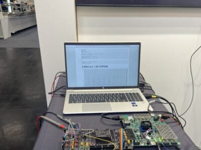
“In all three areas we have customers who want samples,” he said. “We are going for tapeout now for samples in May – HF etch vertical equipment in back end on top of the 180nm ASIC process.” This is built at SMIC in China.
“We have had to invent completely new sensor structures that will work reliably when made in a standard CMOS fab line, which means that they need to work with large residual stress and large process tolerances. These have taken years to perfect but now we have working NEMS in silicon so we are filing ten patent families that between them protect more than 100 inventions,” said Josep Montanyà, Founder and CEO of Nanusens. “Now we can safely start showing them to customers across a wide range of application areas as we have disruptively better solutions for inertial and pressure sensing, ultrasound, microphones and magnetometers, among others. We have many more patents to file over the coming years for yet more novel sensors.”
Nanusens is VC funded by Inveready, Caixa Capital Risc and Dieco Capital as well as several, ultra-high net worth investors. . It leverages the research and expertise developed by the founders’ previous company, Baolab Microsystems, and has research in Barcelona, Spain and China.
Other articles on eeNews Europe
- Embedded boom shields AMD from consumer collapse
- Sondrel IPO sees biggest UK chip deal since ARM
- Infineon commissions new power semiconductor plant in Hungary
- ARM licenses hypervisor for IoT virtual hardware
 If you enjoyed this article, you will like the following ones: don't miss them by subscribing to :