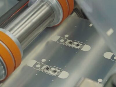
imec charts path beyond 1nm
Belgian research lab imec has charted the path to semiconductor process technology and chip design below 1nm down to the A2 two angstrom generation.
“We are convinced that Moore’s Law will not stop, but there will be many approaches that will all contribute,” said Luc van den Hove, CEO of imec at the Futures conference.
- imec builds working forksheet transistors for 2nm, 1n
- Intel charts path to 1nm – video
- imec resents ‘n-over-p’ complementary FET proposal
He points to several generations of device architecture, evolving from FinFET devices to forksheet and atomic channel devices, as well as new materials and the introduction of high NA lithography systems by ASML which takes many years. The prototype NA systems being installed now will see commercial roll out in 2024.
“We are confident that the lithography tools will be there to extend Moore’s Law well beyond the equivalent 1nm generation. But we will need to develop new device architectures. This will allow the shrinking of a standard cell,” he said.
FinFET has been the workhorse from 10nm down to 3nm. “From 2nm gate all around architectures, built of a stack of nanosheets, will be the most likely concept.”
He points to the forksheet architecture developed at imec. This allows us to put the n and p channel closer together with a barrier material. This will be an option to extend gate all around beyond 1nm. Then you can put the n and p channel on top of each other for further scaling and we believe we have developed the first versions of these.”
Then there are new materials using tungsten or molybdenum that can provide gate lengths of a few atoms for the A10 (1nm) processes in 2028 and below to structures with four Angstrom (A4) in 2034 and two Angtroms (A2) in 2036.
“We recently demonstrated first versions of these atomic channel devices. These will bring us to the sub 1nm generations,” he said.
- Applied upgrade supports backside power and GAA transistors
- Delivering power from the back of a chip
“But we also need to improve the performance of the interconnect. One interesting option is to move the power delivery to the back of the wafer. This leaves more design flexibility for the interconnect on the front side.
“All of this results in scaling for the next fifteen to twenty years,” he said.
To realise the benefits of all these we need a paradigm shift to more domain specific architectures, he says. Future system on chip devices will be integrated as a 3D stack of chips using through silicon via (TSV) and microbump technologies, for example stacking an SRAM memory for the L1 cache right on top of the core logic and using chiplets with different process technologies for different tasks. This leads to multiple 3D chips can be connected on a silicon interposer.
“We have been developing all these enabling technologies that are gradually being picked up by industry as we speak,” he said.
“We need to take into account the sustainability of manufacturing of these devices, the electricity use, the water, the chemicals. In optimising these processes it is not enough to look at the performance, power and area but we have to take into account the environmental aspects of these technologies,”
Other articles on eeNews Europe
- World’s largest commercial drone deployment uses German tech
- Micron to ship 232-layer 3D-NAND memory
- GlobalFoundries launches innovation lab
- Apple looks to e-ink displays for foldable phones
- Old fabs never die – Renesas reopens fab for 300mm silicon power
- TI breaks ground on 300mm US fab
 If you enjoyed this article, you will like the following ones: don't miss them by subscribing to :