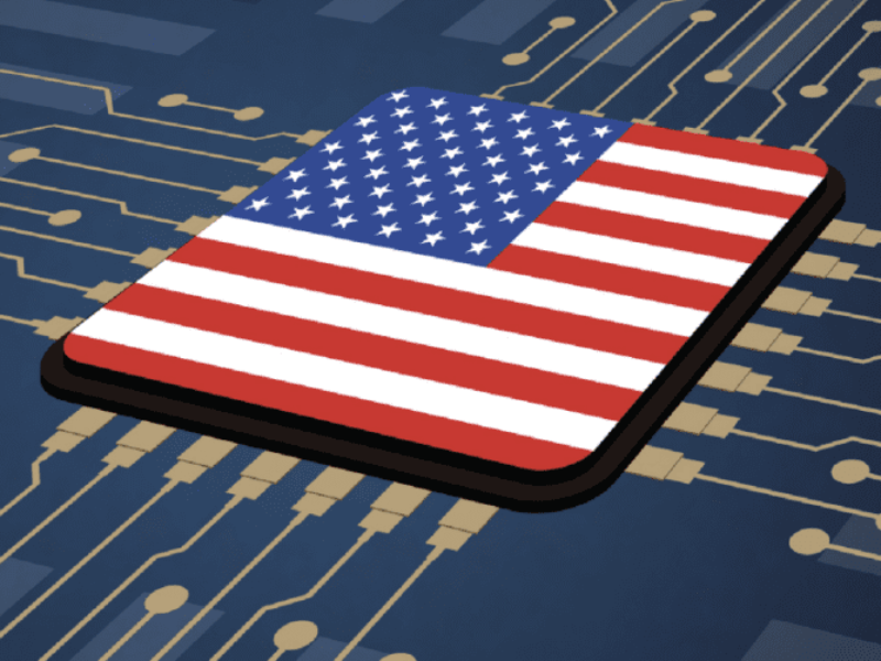
Pitch opens for US $285m digital twin semiconductor centre
The US government has opened applications to build and host the $285m Digital Twin and Semiconductor Manufacturing USA Institute.
A Notice of Funding Opportunity (NOFO) is seeking proposals for a distributed CHIPS Manufacturing USA institute focused on digital twin technology for the semiconductor industry as first detailed by eeNews Europe in February.
Digital twins are virtual models that mimic the structure, context, and behaviour of a physical counterpart. The institute will focus on the development, validation, and use of digital twins for semiconductor manufacturing, advanced packaging, assembly, and test processes.
The CHIPS Manufacturing USA institute is expected to use integrated physical and digital assets across a regionally diverse network and will join an existing network of seventeen Manufacturing USA institutes.
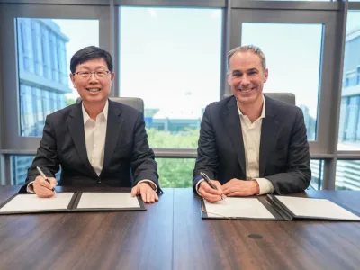
Siemens is expected to be a key contender for the institute, having developed digital twin modelling software and partnered with Intel to develop digital twins of silicon fabs.
- US looks to $200m CHIPS digital twin manufacturing institute
- Intel signs Siemens for fab digitalisation
- Siemens, UL team for first digital twin certification
Unlike traditional, physical research models, digital twins in the cloud enable collaborative design and process development by engineers and researchers across the country, creating new opportunities for participation, speeding innovation, and reducing costs of research and development. Digital twin-based research can also tap into AI to help accelerate the design of new U.S. chip development and manufacturing concepts and significantly reduce costs by improving capacity planning, production optimization, facility upgrades, and real-time process adjustments.
Funded activities are expected to include basic and applied research related to semiconductor digital twin development; establishing and supporting shared physical and digital facilities; industry-relevant demonstration projects; and workforce training.
“Digital twin technology will help transform the semiconductor industry,” said Laurie Locascio, Under Secretary of Commerce for Standards and Technology and National Institute of Standards and Technology (NIST) Director.
“This historic investment in the CHIPS Manufacturing USA institute will help unite the semiconductor industry to unlock the enormous potential of digital twin technology for breakthrough discoveries. This is a prime example of how CHIPS for America is bringing research institutions and industry partners together in public private partnership to enable rapid adoption of innovations that will enhance domestic competitiveness for decades to come.”
This follows the US pulling pack on other CHIPS Act R&D as the funding has been oversubscribed.
“Digital twin technology can help to spark innovation in research, development, and manufacturing of semiconductors across the country – but only if we invest in America’s understanding and ability of this new technology,” said Secretary of Commerce Gina Raimondo.
“This new Manufacturing USA institute will not only help to make America a leader in developing this new technology for the semiconductor industry, it will also help train the next generation of American workers and researchers to use digital twins for future advances in R&D and production of chips,” she said.
“CHIPS R&D is about making sure American manufacturers can continue to succeed and thrive. Digital twin technology can accelerate the costly and time-consuming work to develop the next generation of robust manufacturing for this extraordinarily complicated product,” said Arati Prabhakar, Assistant to the President for Science and Technology and Director of the White House Office of Science and Technology Policy.
 If you enjoyed this article, you will like the following ones: don't miss them by subscribing to :