Power limits the trillion transistor era say Intel, Tesla
Both Intel and Tesla have highlighted the challenges of power management that will limit the coming trillion transistor era.
That era is already approaching, with the Cerebras AI processor array on a wafer with 1.2tn transistors, and Tesla’s DoJo AI training tile (below) with 1.25tn transistors on a wafer substrate in one package. These designs highlight the move to more system-level chip designs, and also the power challenges.
Intel has been addressing this partly through the development of backside power, where power is delivered via traces on the back of a die and through power vias. This allows more space on the top side for signal lines and interconnect and reduces the power losses when the chip, or chiplet, is flipped over to mount on a substrate.
“The wafer foundry is giving way to the systems foundry – the system is becoming the advanced packaging of the future,” said Pat Gelsinger, CEO of Intel, speaking at the HotChHips conference this week. “Power density and power delivery are key. Every chip today is limited by power, and the system problems of today will become the chiplet problems of tomorrow,” he said.
Intel has worked with imec in Belgium over the last decade on this technology as one of the four pillars for the coming trillion transistor era for system-level chip design.
Also at the conference, the lead AI architect at electric car maker Tesla highlighted the power challenges he faces when considering chips from a system level.
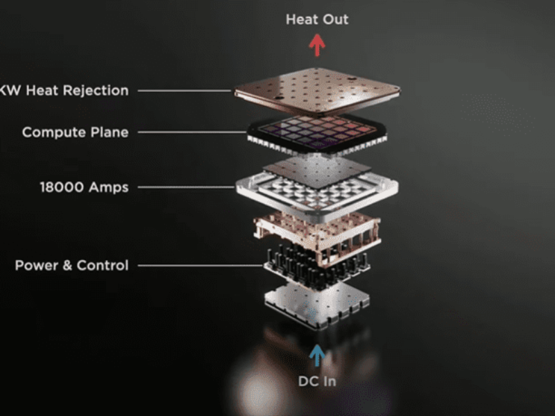
Tesla’s DoJo AI supercomputer is built around tiles of a 5 x 5 matrix of its D1 processors but this tile of 25 processors is limited by the power envelope of 10 to 15kW, says Ganesh Venkataramanan, senior director of autopilot hardware at Tesla.
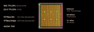
Each of the 400W D1 processors has 50 billion transistors, or 1.25bn transistors when mounted on a wafer using TSMC’s 2.5D fanout process to create what Tesla called a tile. These tiles, first described at Tesla’s AI Day in 2021, are used to train the machine learning framework used in its autopilot self driving software.
“The traditional hierarchy is chip to package to board to box to rack but walking through this hierarchy we lose tremendous bandwidth and latency, and the amount of energy for a calculation has to be considered across the hierarchy,” he said.
Tesla’s D1 processor for its AI supercomputer
“The chip design industry has been innovating tremendously to mitigate this, this is why the chips are reticule sized and then we extend this with silicon interposers and multi-chip modules. But what this causes is growth in power consumption. The GPU trend for power has grown astronomically, from 300W in 2014 to 700W in 2022,” he said.
This led to dark silicon, where parts of a chip are switched off to reduce the overall power consumption. But the immense challenges of AI means every piece of logic in the chip will be used, he said.
“This leads to another issue which is cooling difficulties and leads to solutions that are big and bulky with heatsinks so our systems also grow so the system gets pried apart in to racks and boxes,” he said.
“What we need is a system level view and that’s what led to us looking at this from first principals, for project DoJo. DoJo D1 was just the starting point, we started to think about how to get around the hierarchies,” he said.
“We developed the system on wafer with TSMC where we can reconstruct known good die on the wafer with fanout. This required other innovations, with vertical power delivery vertical, using the fanout layers. What we found was the vertical has good impedance and frequency response so we built more of the system a vertical fashion. This made the wafer sized training tile possible with 25 D1 die without requiring external switches,” he said.
“Once we have the compute tile and training tile, we can build an entire datacentre out of these training tiles,” he said.
The 25 die on the training tile are just the start, and he hints of larger systems to be discussed at Tesla’s AI day in September.
Other technologies for tackling the power challenge were also discussed at the conference having been launched last year.
When chips, or chiplets, are flipped over to place on a substrate, this can enable the use of photonic connections to boost the bandwidth and reduce the power consumption. These photonic interfaces can be built into the chiplets to provide high performance links with lower power consumption.
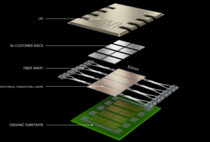
Lightmatter’s passage programmable photonic substrate for the trillion transistor era
Lightmatter detailed its programmable photonic substrate at the conference for just this application, with transistors and photonics integrated side-by-side provide a simple, yet powerful interface that facilitates dynamic reconfiguration of the communications topology.
SerDes signals from chiplets can be directly modulated onto waveguides, using standards such as UCIe which Gelsinger Intel cites as key for future integration of devices in a package ot reach the trillion transistor target.
Dynamic topology reconfiguration capability with algorithms that automatically compute the shortest distance between two communicating sites and communication error detection uses cyclic redundancy checks with a dynamic choice of communication protocols between PAM2, PAM4, or PAM8.
- Photonic interconnect for wafer-scale chips
- Optical processing AI startup launches 4U accelerator
- Broadcom, Tencent to commercialise co-packaged 25Tbit optical switch
The move to system level chip systems with a trillion transistors in a package will also have an impact on the design tools. “We are going to need the next generation of EDA tools, now its going to have to synthesize this hardware system and software across multiple domains so that will be a whole new class of EDA tools to tackle these system problems at scale,” said Gelsinger at Intel.
www.intel.com; www.tesla.com/ai; www.lightmatter.com; www.hotchip.org
Other articles on eeNews Power
- Origami fabric generates electricity from air moisture
- Faraday and NREL team for EV battery research
- Britishvolt gigafactory CEO steps down
- Danfoss completes takeover of power expert Semikron
- Infineon signs 200mm SiC wafer deal with II-VI
 If you enjoyed this article, you will like the following ones: don't miss them by subscribing to :