TSMC in talks about chiplet packaging in Arizona
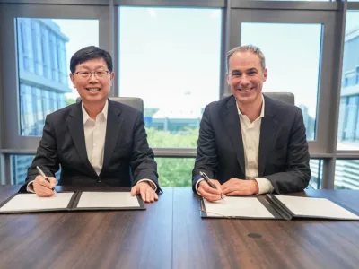
TSMC and the State of Arizona are in talks about setting up advanced chip packaging facilities in the state, according to state governor Katie Hobbs. This would be an addition to the plan for two wafer fabs now being constructed and equipped in Phoeniz, Arizona.
“Part of our efforts at building the semiconductor ecosystem is focusing on advanced packaging, so we have several things in the works around that right now,” Reuters quoted Hobbs saying on the sidelines of a US-Taiwan supply chain forum held in Taipei, Taiwan.
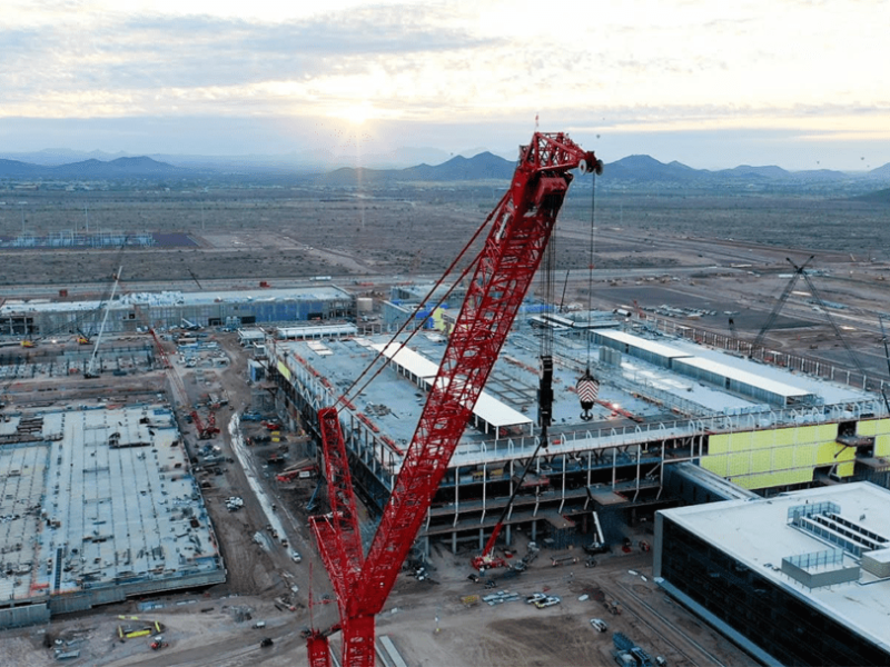
TSMC’s plan of record so far is to spend about US$40 billion to build two wafer fabs on a campus in Phoenix, Arizona. The first shell is complete and has started receiving equipment (see TSMC raises Arizona fabs’ budget to $40 billion).
However, TSMC announced in July that it would have to push back the start of production on the N4 node at the first fab from 2024 to 2025 due to a lack of staff with the skills to hook up the machinery and prepare it for manufacturing. The second fab is due to start manufacturing 3nm silicon in 2026. It has also reportedly started telling is equipment suppliers more generally to slow down on sending chipmaking equipment to multiple sites because of a slowness in the market (see TSMC sees headwinds, flips to 10 percent decline forecast).
Concerns were raised recently in the US that despite an effort to ramp the ability to manufacture leading-edge wafers in the US, many of those wafers would have to be sent to Taiwan or elsewhere in southeast Asia to be packaged. The purpose of US policy on semiconductors and such things as the US Chips Act is to reduce US reliance on southeast Asia for semiconductor components.
The Phoenix Arizona campus is large enough that it could eventually accommodate six fabs (see TSMC planning for six wafer fabs in Arizona) so there is the possibility that one or more plots could be reserved for advanced packaging facilities.
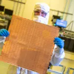
TSMC rival Intel has been claiming that its internally developed chiplet packaging capability is one of the technologies that could help it catch up with TSMC in semiconductor component manufacturing (see Intel tips glass substrate for chiplet packaging).
Related links and articles:
Intel tips glass substrate for chiplet packaging
The US needs to generate, retain more chip workers
TSMC raises Arizona fabs’ budget to $40 billion
TSMC planning for six wafer fabs in Arizona
 If you enjoyed this article, you will like the following ones: don't miss them by subscribing to :