ST builds digital twin of Crolles fab
STMicroelectronics has built a digital twin of its fab in Crolles, France, to monitor and optimise equipment.
The company is using its STM32 32bit microcontrollers with embedded AI to monitor fab equipment and automated transport systems. This is combined with multiple data sources in a digital twin that allows predictive maintenance and system optimisation, says Philippe Magarshack, Group Vice President of the Group Vice President of Strategic Technology & System Architecture in the Microcontrollers and Digital ICs Group (MDG) group at ST. He is also vice-president of the Minalogic Collaborative R&D Cluster in Grenoble.
“Industry 4.0 applications are very diverse and require sophisticated CPS hardware and software, from security, cloud, security, wireless and RTOS,” said Magarshack in a keynote on cyberphysical systems (CPS) at the DATE 2021 conference. “In smart factories all production steps are digitally mapped in a digital twin and connected. At ST we are not only designing products for Industry 4 .0 but using these techniques. Several hundreds of steps in a fab with multiple parameters so it is fundamental to collect and analyse in real time all these parameters.”
Running 6300 wafers per week the 300mm fab at Crolles generates 3TB of data per day. ST is using three AI techniques for monitoring wafers and equipment. Advanced defect classification (ADC) automatically classifies wafer defects with CNN neural network pattern matching so that corrective action in real time and defects are caught before other processes are added in. Then there is equipment fault detection. Instead of measuring a single temperature the complete curve is captured and compared against the golden curve. This allows real time modelling and decision making to optimise productivity, says Magarshack.
Next: Building a digital twin
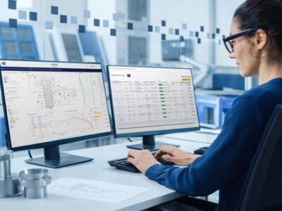
All the data is collected in a factory level digital twin as a system of systems. There are 600 process steps for every wafer with a cycle time 12 weeks, and 150 robot vehicles each travel 45km per day moving wafer lots between equipment with 60,000 transports per day. The twin is a 3D model of the equipment with traffic simulation and fab process optimisation tools.
“Having a digital twin of a fab enables many optimisations and allows us to anticipate the performance of many combinations of process that would be impossible to carry out in real life,” said Magarshack. This also includes the high level models of the sensors and system-on-chip controllers. “CPS devices are at the heart of smart factories and the data generated for digital twins, and we extend SoC validation to factory level use cases and we use it in our own factories,” he said. “The SoC digital twin gives us capability to peek and poke inside a chip for testing unreachable areas and allows us to inject errors anywhere in the system to see what would happen. A wireless network co-simulation of the CPS using the actual embedded software and simulated RF link to test in a factory before they are deployed. These advanced high level models are instrumental in development and are useful even for products in the field.”
The company is developing a next generation of vibration sensor with its STM32WB controller with AI detection that it will install in fabs in the future with a smaller form factor. But it is not just the AI that is important but the data cleaning and semantics of test.
“We are developing a roadmap with specific AI accelerators and these are based on our own architecture developed in internally in ST as we have low power and an understanding of the applications and these will come out in the next year to 18 months,” said Magarshack.
“The emphasis is on detecting and understanding the weak signals. The image of the wafers and their classification is a confined set of problems. We started the journey a year or two ago of identifying single sources of data and we are 20 percent of the way to getting the full value from the data generated each day,” he said.
“We probably have two or three more years to go to get the full benefit but the next big step will happen when we can combine the information form multiple sources. This is difficult as these have different semantics for defects and different causes of defects and so are not easily connected to each other.
“The next challenge for the industry is to come up with a reference data model that can be applied across the board. For example in final test you have automatic test pattern generation (ATPG) with test vectors identifying a short between two lines of metals, but this does not align with the image based classification tool so we need to think about a body of defects and this should be recognised acrosss the various sources of test.
“That’s one area for industrial attention,” he said. “80 percent of the work is in the data cleaning, 20 percent on the algorithms and AI itself so the data cleaning needs attention and some of that is implementable and that’s an area of research I would recommend.”
Related digital twin articles
- €30M DIGITAL FACTORY PLAN FOR PARIS
- EDGE AI STARTUP RAISES $10M FOR ELECTRONICS MANUFACTURING
- FIRST INTERNATIONAL STANDARD
- WIND RIVER IN TWIN MOVE
Other articles on eeNews Europe
- Globalfoundries plans to boost production
- Electronics eats the car industry
- Europe’s semiconductor challenge
- Bosch looks to AIoT as revenue falls
- European project for commercial silicon quantum processor
 If you enjoyed this article, you will like the following ones: don't miss them by subscribing to :
eeNews on Google News


